Timing 201 #7: The Case of the Dueling PLLs – Part 1
Author: Kevin G. Smith
Introduction
RF and microwave frequency synthesizers often employ multiple connected PLLs. These architectures trade off complexity in favor of improved phase noise, smaller frequency step size, and faster switching [1]. In timing applications we may also employ multiple PLLs to combine timing functions and/or shape phase noise.
For example, the white paper, “Optimizing Clock Synthesis in Small Cells and Heterogeneous Networks”, describes Silicon Labs’ DSPLL dual-loop architecture as used in the Si538x wireless jitter attenuators intended for small cell applications [2]. This particular approach is a nested dual-loop as opposed to a cascaded (concatenated) dual-loop. There are definite advantages to this implementation and some important considerations.
One consideration is the necessary bandwidth relationship between the inner and outer loops. This topic leads to the play on words in the main title of this blog post, The Case of the Dueling PLLs. A second consideration is the difference in how one analyzes the phase noise for such an architecture, which arises from the fundamental difference between these two approaches as explained below.
General Motivation for a Dual-Loop PLL Architecture
As you may recall from a previous blog post, there are two basic PLL clock applications [3]:
- Clock Generator (aka clock multiplier, frequency multiplier, etc.)
- Jitter Attenuator (aka jitter cleaner)
Low noise references are input to clock generators, which are usually wide bandwidth (e.g., 100s kHz to MHz). By contrast, jittery clocks are input to jitter attenuators, which are usually narrow bandwidth on the order of kHz or less.
But what if your clock application requires both functions? The most straightforward approach is to cascade the two PLLs in series as discussed in the next section.
Cascaded Dual-Loop PLL Architecture
The figure below, taken from the cited white paper, illustrates a single-chip, cascaded dual-loop architecture. (Note that this sense of the term cascade is different from classic control system terminology. Here we mean two PLLs concatenated or in series.)

In this case, the left hand PLL1 with an analog Voltage Controlled Xtal Oscillator (VCXO) is used as a narrow band jitter attenuator stage. The jitter attenuated clock signal is then input to the right hand PLL2, which is used as a wide band clock generator stage. The VCXO need not be very high in frequency but should have good close-in phase noise. This generally means a high Q crystal, which is why this component is typically external to the IC. This necessitates an external control voltage signal to the VCXO.
The on-chip VCO needs to be high enough in frequency so that the divided down clock can yield the necessary output clock frequencies. It also should have low phase noise at high offset frequencies.
This particular example is depicted as all analog with several external filter components and sensitive traces. However, there is no intrinsic reason why a cascaded dual-loop architecture could not be implemented more digitally and with filtering on-chip.
Because the PLLs in the example above are in-series and independent, the total output phase noise can be calculated as a cascade of phase noise processing elements as described in [3].
Nested Dual-Loop PLL Architecture
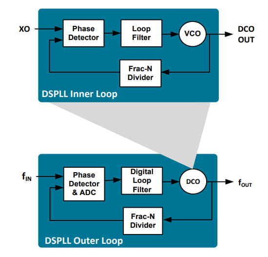
The figure below, also from the cited white paper, illustrates a nested dual-loop architecture. In classic control system terminology, this would actually be considered a variation of a cascade control system. For clarity, I will use the term nested here. Think of it as the PLL equivalent of nested Matryoshka dolls.

In this case, the inner loop (IL) PLL is being used as the “VCO” or rather the Digitally Controlled Oscillator (DCO) of the outer loop (OL) PLL. This is the fundamental difference between these two approaches, which will determine how one calculates the total phase noise.
How does this work?
- The output of the OL digital loop filter modulates the return path of the IL.
- The output of the IL VCO is in fact the fOUT in the diagram. In practice, this output frequency is divided further to yield the necessary output clocks.
What are the advantages to this approach?
In this particular pair of examples, we reduce the number of tuned oscillators from two (VCXO and VCO) down to one (XO and VCO). This eliminates the need for one of the loop filters (be it internal or external) and a sensitive voltage control line, which must otherwise be routed externally. This decrease in components makes for a more compact solution which reduces the overall PCB footprint.
Could you implement a nested dual-loop with a VCXO?
Yes, in principle. There is no intrinsic reason why you couldn’t implement a nested dual-loop architecture that also uses an external VCXO. Such an approach might even make sense if a particular VCXO has better phase noise performance, perhaps at a higher frequency (update rate). However, you would lose the specific advantages discussed previously. This is why the Si538x wireless jitter attenuators do not support an external VCXO.
What exactly is the Duel?
In these types of nested feedback control loops, the inner loop must be faster than the outer loop. If the loop speeds are comparable, then the loops will contend or “duel” with each other.
In PLL terms the inner loop must have a wider bandwidth than the outer loop. This should make intuitive sense if you consider the relative difference in impact of inserting a really slow “DCO” into an otherwise fast PLL versus inserting a really fast “DCO” into an otherwise slow PLL. The former case significantly impacts the PLL and may even have stability or locking issues due to inserted additional delay. By contrast, the latter case is not impacted significantly. This tells us that the inner loop must be the faster (wider bandwidth) clock multiplier and the outer loop must be the slower (narrow bandwidth) jitter attenuator. Further, it tells us that at start-up and during the lock process, we want the inner loop PLL to stabilize and lock before the outer loop.
Another way of thinking about this is to recall that PLLs function as a low pass filter for phase noise arising from any source in the loop, except when they function as a high pass filter to VCO phase noise. For the OL PLL to modulate the IL’s return path without attenuation, the signal must be well within the IL BW.
Incidentally, if you want to estimate one quantity from another, such as frequency step rise time from PLL bandwidth, you may use this relationship:
Tr [10%-90%] * BW [3dB] ≈ 0.35
See for example, Howard Johnson’s discussion in the article, PLL Response Time [5]. Per his article, the time bandwidth product varies from 0.35 to 0.38, depending on whether the PLL behaves closer to a single-pole or double-pole response.
How much faster or wider bandwidth must the inner loop be? In mechanical engineering and process control systems, the differences in nested loop speeds can be relatively small. A mechanical IL may be 5x to 10x faster than a mechanical OL. See for example Danielle Collins’ servo loop article in [6]. However, in timing applications, the difference in bandwidths is typically much greater. Nested dual-loop IL BWs are typically on the order of MHz, whereas OL BWs can be on the order of 10 Hz to 1 kHz, so the ratio is closer to the IL being 1000x to 100,000x faster than the OL.
Note that for Si538x devices, the IL BW is wide (~ 1 MHz), fixed, and optimized. Because it is so wide, there is no jitter attenuation at the device’s XO inputs, i.e., the XA/XB pins. Therefore, we should be careful that noise and interference does not couple into the device via the XO circuit at these pins. This is why we recommend low phase noise XOs to be placed as close as possible to the device so as to minimize PCB trace lengths.
Can this idea be extended?
Yes, in principle. The servo control loop article cited earlier discusses a servo motor control with three nested loops, inside to outside as follows: current feedback, velocity feedback, and position feedback. Similarly, you can “triple nest loop” clock PLLs to shape the phase noise to track select input clocks with different phase noise characteristics over different frequency offsets. However, this particular approach is not utilized by the Si538x devices.
Conclusion
I hope you have enjoyed this Timing 201 article. In the Part 2 follow-up post, I will discuss in more detail how to calculate the phase noise of the nested dual-loop approach using a simplified example.
As always, if you have topic suggestions or questions appropriate for this blog, please send them to kevin.smith@skyworksinc.com with the words Timing 201 in the subject line. I will give them consideration and see if I can fit them in. Thanks for reading. Keep calm and clock on.
Cheers,
Kevin
References
- W. F. Egan, Advanced Frequency Synthesis by Phase Lock. Wiley, 2011. See for example section 7.1 regarding the Two-Loop Synthesizer where two loops interact via a mixer.
- Optimizing Clock Synthesis in Small Cells and Heterogeneous Networks
https://www.skyworksinc.com/-/media/SkyWorks/SL/documents/public/white-papers/Optimizing-Clock-Synthesis-in-Small-Cells-and-Heterogeneous-Networks.pdf
- Timing 101 #11: The Case of the Noisy Source Clock Tree Part 1
https://www.skyworksinc.com/en/Blog/2022/09/Timing-101-11
- Timing 101 #12: The Case of the Noisy Source Clock Tree Part 2
https://www.skyworksinc.com/en/Blog/2022/09/Timing-101-12
- H. Johnson, PLL Response Time, High-Speed Digital Design Online Newsletter: Vol. 15 Issue 04,
http://www.sigcon.com/Pubs/news/15_04.htm
- D. Collins, Why is the bandwidth of a servo control loop important?, April 20, 2017, https://www.motioncontroltips.com/why-is-the-bandwidth-of-a-servo-control-loop-important/
[Note: This blog article was originally posted online in November 2020. It has been lightly edited, and updated to reflect Skyworks Solutions’ acquisition of Silicon Labs’ Infrastructure and Automotive business, completed on July 26, 2021.]

By Kevin G. Smith
Sr. Principal Applications Engineer


