The topic of wander covers a lot of material. Even introducing the highlights will take more than one blog article. In this first post, I will discuss the differences between wander and jitter, the motivation for understanding wander, and go in to some detail regarding a primary wander metric: MTIE or Maximum Time Interval Error. Next in this mini-series, I will discuss TDEV or Time Deviation. Finally, I plan to wrap up with some example lab data.
Some Formal Definitions
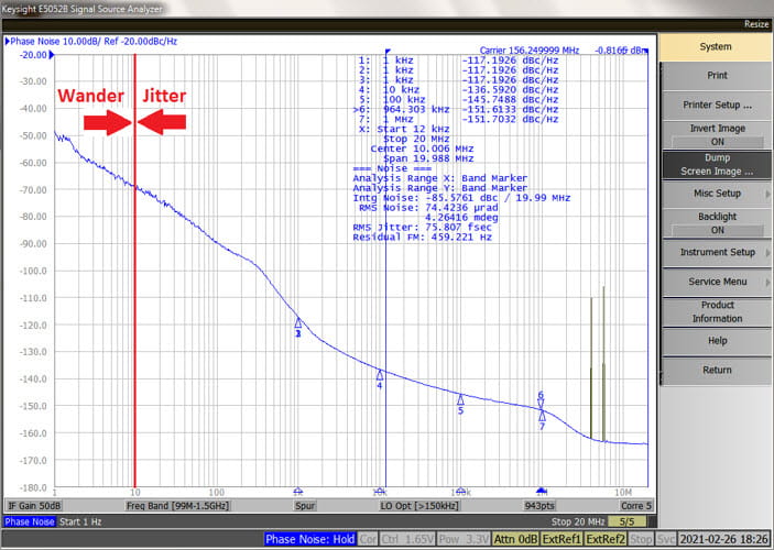
The 10 Hz dividing line, in common use today, has been used in synchronous optical networking (SONET) and synchronous digital hierarchy (SDH) standards for years. For example, ITU-T G.810 (08/96) Definitions and terminology for synchronization networks [1] defines jitter and wander as follows.
4.1.12 (timing) jitter: The short-term variations of the significant instants of a timing signal from their ideal positions in time (where short-term implies that these variations are of frequency greater than or equal to 10 Hz).
4.1.15 wander: The long-term variations of the significant instants of a digital signal from their ideal position in time (where long-term implies that these variations are of frequency less than 10 Hz).
Similarly, the SONET standard Telcordia GR-253-CORE [2] states in a footnote
Short-term variations” implies phase oscillations of frequency greater than or equal to some demarcation frequency. Currently, 10 Hz is the demarcation between jitter and wander in the DS1 to DS3 North American Hierarchy.
Wander and jitter are clearly very similar since they are both “variations of the significant instants of a timing signal from their ideal positions in time”. They are also both ways of looking at phase fluctuations or angle modulation (PM or FM). Their only difference would appear to be scale. However, that can be a significant practical difference.
Consider by analogy the electromagnetic radiation spectrum, which is divided into several different bands such as infrared, visible light, radio waves, microwaves, and so forth. In some sense, these are all “light”. However, the different types of EM radiation are generated and detected differently and interact with materials differently. So it has always made historical and practical sense to divide the spectrum into bands. This is roughly analogous to the wander versus jitter case in that these categories of phase fluctuations differ technologically.
Why 10Hz?
So, how did this 10 Hz demarcation frequency come about? Generally speaking, wander represented timing fluctuations that could not be attenuated by typical PLLs of the day. PLLs in the network elements would just track wander, and so it could accumulate. Networks have to use other means such as buffers or pointer adjustments to accommodate or mitigate wander. Think of the phase noise offset region, 10 Hz and above, as “PLL Land”.
Things have changed since these standards. Back in the day it was uncommon or impractical to measure phase noise below 10 Hz offset. Now phase noise test equipment can go down to 1 Hz or below. Likewise with digital and FW/SW PLLs it is possible to have very narrowband PLLs which can provide some “wander attenuation”. Nonetheless, 10 Hz offset remains a useful dividing line and lives on in the standards.
Wander Mechanisms
Clock jitter is due to the relatively high frequency inherent or intrinsic jitter of an oscillator or other reference ultimately caused by flicker noise, shot noise, and thermal noise. Post processing by succeeding devices such as clock buffers, clock generators, and jitter attenuators can contribute to or attenuate this random noise. Systemic or deterministic jitter components also can occur due to crosstalk, EMI, power supply noise, reflections etc.
Wander, on the other hand, is caused by slower processes. These include lower frequency offset oscillator and clock device noise components, plus the following.
- Slight initial differences in frequency and phase between clocks
- Slow changes in frequency and phase between clocks due to environmental differences such as temperature or vibration
- Frequency and phase transients caused by switching clocks
For a good discussion of some of these wander mechanisms and their impact on a network, see [3].
Since wander mechanisms are different, at least in scale, and networks tend to pass or accumulate wander, industry has focused on understanding and limiting wander through specifications and standards.
Wander Terminology and Metrics
You may recall the use of the terms jitter generation, jitter transfer, and jitter tolerance. These measurements can be summarized as follows.
- Jitter Generation - How much jitter is output if a jitter-free input clock is applied
- Jitter Tolerance - How much input jitter can be tolerated without affecting device performance
- Jitter Transfer - How much jitter is transferred if a jittery input clock is applied
These definitions generally apply to phase noise measurements made with frequency domain equipment such as phase noise analyzers or spectrum analyzers. They are useful when cascading network elements.
By contrast, wander is typically measured with time domain equipment. Counterpart definitions apply as listed below.
- Wander Generation - How much wander is output if a wander-free input clock is applied
- Wander Tolerance - How much input wander can be tolerated without affecting device performance
- Wander Transfer - How much wander is transferred if a wandering input clock is applied
Wander has its own peculiar metrics too. In particular, standards bodies such as the ITU rely on masks that provide limits to wander generation, tolerance, and transfer based on one or both of the following two wander parameters. See for example ITU-T 8262 [4].
- MTIE (Maximum Time Interval Error)
- TDEV (Time Deviation)
Very briefly, MTIE looks at peak-peak clock noise over intervals of time as we will discuss below. TDEV is a sort of standard deviation of the clock noise after some filtering. We will discuss TDEV next time.
Before going into detail about MTIE, let’s discuss the foundational measurements Time Error and TIE (Time Interval Error). These are both defined in the previously cited ITU-T G.810.
Time Error (TE)
The Time Error function x(t) is defined as follows for a measured clock generating time T(t) versus a reference clock generating time Tref(t). The frequency standard Tref(t) can be regarded as ideal, i.e., Tref(t) = t.
x(t) = T(t) – Tref(t)
Time Interval Error (TIE)
Similarly, the Time Interval Error function is then defined as follows, where the lower case Greek letter “tau” is the time interval or observation interval.
TIE(t;τ) = [T(t + τ) – T(t)] - [Tref(t + τ) – Tref(t)] = x(t + τ) – x(t)
Maximum Time Interval Error (MTIE)
MTIE measures the maximum peak-peak variation of TIE for all observation times of length tau = ntau0 within measurement period T. ITU-T G.810 gives the following formula for estimating MTIE
MTIE (nτ0) @ max1≤k≤N-n [maxk≤i≤k+n (xi) – mink≤i≤k+n (xi)], n = 1, 2, … N-1
Where:
τ0 = sample period
τ = observation time
T = measurement period or (N-1)τ0
xi = i-th time error sample
xppk = peak-to-peak xi within the k-th observation
MTIE(τ) = maximum xpp for all observations of length τ within T
The sampling period represents the minimum measurement interval or observation interval. There are many terms used in the industry that are synonymous and should be recognizable in context: averaging time, sampling interval, sampling time, etc. This could mean every nominal period if you are using an oscilloscope to capture TIE data. However, most practical measurements over long periods of time are only sampling clocks. This would correspond to a frequency counter’s “gate time”, for example, if post-processing frequency data to obtain phase data.
An MTIE Example
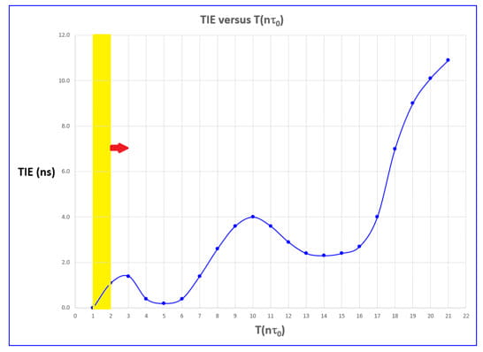
It’s better to show you the general idea at this point. Below, I have modified an illustration after ITU-T G.810 Figure II.1 and indicated a tau=1tau0 observation interval or window as it is moved across the data. (The data are for example only and do not come from the standard. I have also started at 0 as is customary to show changes in Time Error or phase since the start of the measurement.) The initial xppk peak-peak value at the location shown is about 1.1 ns – 0 ns = 1.1 ns.

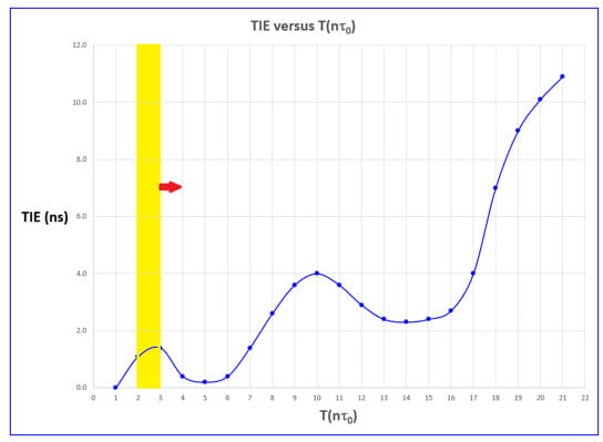
Now slide the tau=1tau0 observation interval right and the next xppk peak-peak value is 1.4 ns – 1.1 ns = 0.3 ns.

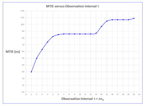
If we continue in this vein to the end of the data, we will find the worst case to be between 17tau0 and 18tau0 and the value is 7.0 ns – 4.0 ns = 3.0 ns. Therefore, the MTIE for tau=1tau0 is 3.0 ns.
I have calculated the MTIE plot for this dataset in the attached Excel spreadsheet 201-9_Example_MTIE_Calcs.xlsx. Note that the first value in the plot is 3 ns as just mentioned. This is a relatively simple example for illustration only. MTIE data typically spans many decades and are plotted against masks on logarithmic scales.

However, even this simple example suggests a couple of items to note about MTIE plots:
- MTIE plots always increase monotonically.
This is because MTIE acts as a max peak detector over an interval. Larger variations in the data are encompassed as the observation interval increases.
- Large transients will mask smaller transients.
Again, a max peak detector will not reveal smaller variations.
Why is MTIE Useful?
MTIE is a relatively computation intensive measurement. So what good are these type of plots? There are at least two good reasons besides standards compliance:
MTIE can be used to size buffers. As noted here [3]:
Buffer size > MTIE (τ) implies that overflow/underflow [is] unlikely in any interval < τ
Buffer size = MTIE (τ) implies that overflow/underflow could occur approx. every τ seconds
MTIE indicates phase behavior. [4]
a. Plateaus correspond to a phase shift.
b. Ramps correspond to a phase slope (frequency offset).
Conclusion
In this post, I have discussed the differences between wander and jitter, the motivation for understanding wander, and delved in to MTIE, a wander metric important to standards compliance and useful in sizing buffers.
I hope you have enjoyed this Timing 201 article. In the Part 2 follow-up post, I will discuss another important wander metric: TDEV or Time Deviation.
As always, if you have topic suggestions or questions appropriate for this blog, please send them to kevin.smith@skyworksinc.com with the words Timing 201 in the subject line. I will give them consideration and see if I can fit them in. Thanks for reading. Keep calm and clock on.
Cheers,
Kevin
References
- ITU-T G.810 Definitions and terminology for synchronization networks
https://www.itu.int/rec/T-REC-G.810-199608-I/en
- Telcordia GR-253-CORE, Synchronous Optical Network (SONET) Transport Systems: Common Generic Criteria
The official version is orderable but not free from
https://telecom-info.njdepot.ericsson.net/site-cgi/ido/docs.cgi?ID=SEARCH&DOCUMENT=GR-253&.
My old copy is Issue 3, September 2000 but the fundamentals have not changed with the newer issues.
- Understanding Jitter and Wander Measurements and Standards, 2003
http://literature.cdn.keysight.com/litweb/pdf/5988-6254EN.pdf
This old Agilent (now Keysight) document remains a treasure, especially for SONET/SDH jitter and wander. See “Cause of wander” starting on p. 118.
Please note that as of last editing, the Keysight link above appears to be broken. It is retained here for reference. Fortunately, this document is archived on the internet at
https://web.archive.org/web/20170713013258/http://literature.cdn.keysight.com/litweb/pdf/5988-6254EN.pdf.
- ITU-T G.8262 Timing characteristics of a synchronous equipment slave clock
https://www.itu.int/rec/T-REC-G.8262-201811-I/en
- K. Shenoi, Clocks, Oscillators, and PLLs, An introduction to synchronization and timing in telecommunications, WSTS – 2013, San Jose, April 16-18, 2013
https://tf.nist.gov/seminars/WSTS/PDFs/1-1_Qulsar_Shenoi_tutorial.pdf
An excellent tutorial. See slide 12.
- L. Cossart, Timing Measurement Fundamentals, ITSF November 2006.
http://www.telecom-sync.com/files/pdfs/itsf/2006/workshop/05-Cosart.pdf
Another excellent tutorial. See slides 40 – 41.
[Note: This blog article was originally posted online in March 2021. It has been lightly edited, and updated to reflect Skyworks Solutions’ acquisition of Silicon Labs’ Infrastructure and Automotive business, completed on July 26, 2021.]

By Kevin G. Smith
Sr. Principal Applications Engineer


