Timing 201 #12: The Case of the Frequency Scaled Invariant Phase Jitter
Author: Kevin G. Smith
Introduction
If you compare phase noise plots for different output clocks from the same device, where the clock frequencies only differ by a scaling ratio N, you may notice that while the phase noise profiles will generally go up or down by 20*log10(N), the RMS phase jitter will be relatively constant. That is, all else being equal, frequency scaled RMS phase jitter measurements integrated over the same jitter bandwidth will tend to be roughly the same. The first time one encounters this behavior, it may seem a bit counter-intuitive. This observation prompts the subject of this post, “The Case of the Frequency Scaled Invariant Phase Jitter”.
An Example
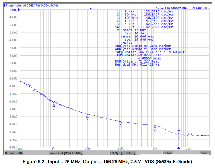
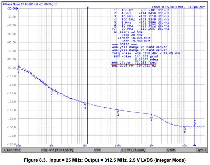
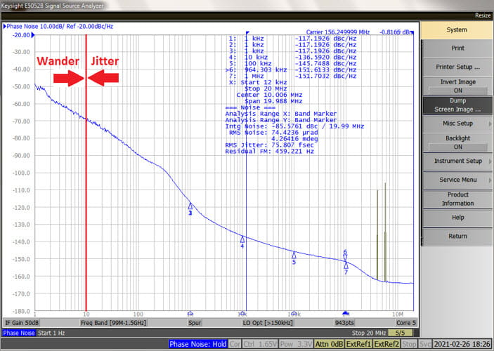
Consider the Skyworks Si5395 jitter attenuator datasheet [1]. Figures 8.2 and 8.3, copied below, conveniently present sample phase noise plots for output clocks 156.25 MHz and 312.5 MHz respectively where the frequency scaling ratio N =2. The input clock is 25 MHz and the output clock format is 2.5 V LVDS in each case.


If we are familiar with the 20*log10(N) rule, we would expect that phase noise would be worse (higher) for the 312.5 MHz clock versus the 156.25 MHz clock by about 20*log10(2) = 6 dB. The overall shape of the example phase noise curves do appear very similar except for the offset frequencies closest in and farthest out. Now let’s compare some of the reported calculations in the upper right hand corner of these plots. (We will discuss how these numbers are calculated later on.)

The difference in the reported Intg Noise is roughly 6 dB as expected. (Inspecting spot phase noise where measured in both plots we see marker differences actually range from 5 to 7 dB in the 12 kHz to 20 MHz jitter bandwidth.) However, the measured RMS phase jitter is very close, 71.227 fs versus 73.518 fs respectively.
This last line in the table is the counter intuitive aspect mentioned in the title of this post. When first encountering phase jitter, we may see higher phase noise and think - ah well there must be significantly higher phase jitter right? It turns out that is not the case. Let’s review the math and the interpretation of these numbers.
Why 20*log10(N) in the First Place?
Dr. William Egan discussed the general behavior of phase noise through synchronous frequency dividers in [2] as follows.
Φc = ΔT*F
Φco = ΔT*Fo = ΔT*Fi/N =
Φci /N
Φo = Φi /N
Where
Φc = phase variation in cycles
ΔT = jitter in seconds
F = signal frequency
N = division ratio
The i and o subscripts denote input and output parameters respectively. The unit of cycles is dropped for the last equation Φo = Φi /N since it is valid as long as both Φo = Φi use the same units.
The power ratio of (Φo/Φi)2 = (1/N)2 so the phase noise change in dB is -20*log10(N), i.e. phase noise reduces if divided by N > 1. Similarly, if we take N as multiplication as in Φco = Φci *N then the phase noise change in dB is 20*log10(N), i.e. phase noise increases if multiplied by N > 1.
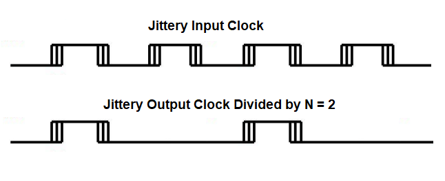
The clock waveforms illustrated below may help provide some intuition. Here we have a jittery clock applied as an input to a noiseless frequency divider that divides the clock by N = 2. There are several points intended to be suggested by this simple illustration:
- Timing jitter is observed at the clock edges.
- A noiseless divider will not add jitter.
- Timing jitter for the divided clock corresponds to reduced output phase variation since the nominal clock period has doubled.

Phase Jitter Calculations Review
Phase noise is integrated over the integration bandwidth as integ[10^(ℒ (f)/10)] and reported on the Keysight E5052B phase noise analyzer for example as
Intg Noise (Integral Phase Noise) = 10*log10{integ[10^(ℒ (f)/10)]} [dBc]
This is just the integral of the SSB phase noise as displayed on the instrument. The units of this operation are interpreted as dBc since we are multiplying units [dBc/Hz] * [Hz].
The RMS phase noise in radians accounts for both sidebands by taking the RSS as follows.
RMS Noise = sqrt{2*integ[10^(ℒ (f)/10)]} [rad]
This can also be written as
RMS Noise = sqrt{2*10^(Integral Phase Noise/10)} [rad]
So using the 156.25 MHz plot example, we expect RMS Noise = sqrt{2*10^(-86.1174/10)} [rad] = 69.9272 μrad which matches the plot results.
RMS Noise in radians is converted to RMS Noise in degrees by multiplying by (180°/π).
Again using the 156.25 MHz plot numbers, if RMS Noise = 69.9272 μrad then that equates to 69.9272E-6*(180°/π) = 4.00653 mdeg. This is consistent with the plot except for some rounding error.
Finally, RMS jitter in seconds is converted from RMS Noise [rad] as follows by multiplying by Tc/(2π) [sec/rad].
RMS Jitter = RMS Noise / (2*π*fc) = Tc * RMS Noise / (2*π) [sec]
Per the 156.25 MHz plot example,
RMS Jitter = 69.9272 μrad / (2*π*156.25 MHz) = 71.227 fs.
Again, this matches the plot results.
Why Then is Phase Jitter Scaling Frequency Invariant?
Note that the carrier frequency did not enter into the calculations until the last step. Let’s look at what happens if we scale the phase noise everywhere by 20*log10(N) where N is a multiple of fc.
Consider that adding 20*log10(N) everywhere is the linear equivalent of multiplying by
10(20*log10(N)/10) = 10(2*log10(N)) = 10(log10(N^2)) = N2
Therefore, RMS noise increases as follows.
RMS Noise = sqrt{2*N2*10^(Integral Phase Noise/10)}
RMS Noise = N*sqrt{2*10^(Integral Phase Noise/10)}
Since RMS Jitter = RMS Noise / (2*π*(N*fc)) where the new carrier frequency is N*fc, we can write
RMS Jitter = N*sqrt{2*10^(Integral Phase Noise/10)}/ (2*π*(N*fc))
The “N”s cancel out and we are left with the expressions we had before scaling the phase noise, i.e.
RMS Jitter = RMS Noise / (2*π*fc) = Tc * RMS Noise / (2*π) [sec]
Therefore RMS (phase) jitter is scaling frequency invariant.
Interpreting Phase Jitter
In the time domain, the term absolute jitter refers to measuring the timing differences between a practical clock’s edges versus an ideal clock’s edges. This is also referred to as Time Interval Error (TIE). This jitter metric is edge oriented as opposed to other relative timing jitter metrics that measure the differences between intervals such as period jitter or cycle-to-cycle jitter. Phase noise can be regarded as a measurement of excess phase and jitter regarded as sampled excess phase [3].
Phase jitter is a filtered frequency domain calculation of absolute jitter. As the previous clock waveforms illustration suggests, assuming noise free dividers and all else being equal, then the absolute jitter at each rising and falling edge will be the same. This follows for the filtered frequency domain contributions to the jitter at each edge also.
This frequency scaled invariance is one of the reasons why phase jitter is a valuable concept. It allows us to compare timing devices to first order regardless of output clock frequency. Typical Si5395 Grade E 12 kHz to 20 MHz RMS phase jitter is specified as 71-85 fs for frequencies ranging from 156.25 MHz to 644.531248 MHz.
The second reason that phase jitter is valuable is because it is filtered in the frequency domain. This is very useful when analyzing the impact of reference clock jitter in serial data applications. See for example the related discussion in Skyworks AN1104 [4].
What About Phase Jitter in UI?
Frequency scaled phase jitter is invariant when expressed as an absolute quantity in units of seconds. However, this relationship does not hold when phase jitter is made relative again by expressing it in terms of UI or Unit Interval. The Unit Interval is defined as 1 bit period and is the nominal width of a data eye. See for example, Onsemi AND9075/D [5]. UI and bit time are the same for NRZ data but can differ in general.
Older standards may specify peak-peak and RMS phase jitter in UI. For example, the Telcordia (Bellcore) GR-253-CORE Issue 4, December 2005, “Synchronous Optical Network (SONET) Transport Systems: Common Generic Criteria” specified the SONET jitter generation limit for OC-48 12 kHz to 20 MHz as 0.1 UIpp and 0.01 UIrms. These limits are commonly written as 100 mUIpp and 10 mUIrms [6]. RMS phase jitter in UI is calculated by dividing the RMS phase jitter [sec] by the clock period expressed as [sec/UI].
The 156.25 MHz and 312.5 MHz clock periods can be written as 6.4 ns/UI and 3.2 ns/UI respectively. Therefore, the phase jitter can be calculated in units of UI as follows.
- 156.25 MHz RMS phase jitter: 71.227E-15 [sec] / 6.4E-9 [sec/UI] = 1.113E-5 UI or 11.13 μUI.
- 312.50 MHz RMS phase jitter: 73.518E-15 [sec] / 3.2E-9 [sec/UI] = 2.297E-5 UI or 22.97 μUI.
These phase jitter numbers are a very small fraction of the clock period but are not invariant. Twice the carrier frequency means twice the phase jitter in UI.
Ceteris Paribus (“all else being equal”)
Finally, you may have heard of the Latin phrase “ceteris paribus” which means “all else being equal”. This measurement goal holds true for phase noise plot comparisons in general and for frequency scaled invariant phase jitter in particular.
Generally, frequency scaled invariant phase jitter is observed when the DUT configuration, input and reference clocks, instrument set-up, operating conditions, and output clock formats are identical other than output divider value. This overall observation can hold true even where there are minor variations. For example, careful readers may note that the E5052B IF Gain settings for the 2 example phase noise plots were not identical, being 40 dB in the first instance and 50 dB in the second instance.
However, phase noise (and phase jitter invariance) can be impacted by secondary factors such as instrument floor, aliasing, and AM noise, especially at lower carrier frequencies. These topics have been discussed in previous posts Timing 101 #3: The Case of the Jitterier Divide-Down Clock, Timing 201 #1: The Case of the Phase Noise That Wasn’t - Part 1 and Timing 201 #2: The Case of the Phase Noise That Wasn’t - Part 2.
Summary
The bottom line is that RMS phase jitter is an edge-oriented absolute jitter metric and is expected to be frequency scaled invariant provided the frequency divider does not add significant jitter. If this is not the case, it is worth checking to understand why.
I hope you have enjoyed this Timing 201 article.
As always, if you have topic suggestions or questions appropriate for this blog, please send them to kevin.smith@skyworksinc.com with the words Timing 201 in the subject line. I will give them consideration and see if I can fit them in. Thanks for reading.
Cheers,
Kevin
References
[1] Skyworks, “Si5395/94/92 Data Sheet 12-Channel, Any-Frequency, Any-Output Jitter Attenuator/Clock Multiplier with Ultra-Low Jitter, Rev. 1.2,” Dec. 2021. Accessed: Oct. 30, 2024. [Online]. Available: https://www.skyworksinc.com/-/media/Skyworks/SL/documents/public/data-sheets/si5395-94-92-a-datasheet.pdf
[2] W. F. Egan, "Modeling phase noise in frequency dividers," in IEEE Transactions on Ultrasonics, Ferroelectrics, and Frequency Control, vol. 37, no. 4, pp. 307-315, July 1990, doi: 10.1109/58.56498.
https://ieeexplore.ieee.org/document/56498
<I worked with the late great Dr. “Bill” Egan years ago at another company where he was a collegial and exemplary engineer. His frequency synthesis, PLL, and RF books are models of rigor and clarity and highly recommended.>
[3] A. Sheikholeslami, “ESSCIRC 2019 Tutorials Fundamental Concepts in Jitter and Phase Noise.” Accessed: Oct. 30, 2024. [Online]. Available: https://www.eecg.utoronto.ca/~ali/papers/1-ESSCIRC2019-Tutorial-Ali-Sheikholeslami.pdf.
[4] Skyworks, Application Note “AN1104: Making Accurate PCIe Gen 4.0 Clock Jitter Measurements”, 2021. Accessed: Oct. 30, 2024. [Online]. Available: https://www.skyworksinc.com/-/media/SkyWorks/SL/documents/public/application-notes/an1104-making-accurate-clock-jitter-measurements.pdf.
See page 3, section 2. PCIe Clock Timing Schemes, Jitter Measurement and Correction Methodology.
[5] Onsemi, Application Note “AND9075/D, Understanding Data Eye Diagram Methodology for Analyzing High Speed Digital Signals”, 2015. Accessed: Oct. 30, 2024. [Online]. Available: https://www.onsemi.com/pub/collateral/and9075-d.pdf.
[6] N. Schmitt and D. Grant, “SONET/SDH jitter measurements of high-speed OC-48 optical transceivers,” Lightwaveonline.com, Jun. 14, 2002. Accessed: Oct. 30, 2024. [Online]. Available: https://www.lightwaveonline.com/optical-tech/transmission/article/16653449/sonet-sdh-jitter-measurements-of-high-speed-oc-48-optical-transceivers.

By Kevin G. Smith
Sr. Principal Applications Engineer


