Sept. 01, 202220 Min Read
Timing 101 #1: The Case of the (Apparently) Jittery Jitter Attenuated Clock
Author: Kevin G. Smith
Introduction
Hello and welcome to this inaugural article for Timing 101. My goal is to introduce and review technical topics of interest to board and systems designers who apply timing components or ICs (aka “clock chips”). Clock chips deliver frequency and phase information via clock waveforms, and in some cases packetized time information.
In this post, I will go over a common test set-up measurement situation whose results may be unexpected when one initially encounters jitter attenuators. I will first review some requisite background material, then present the "mystery" and its root cause, and finally suggest an improved test set-up.
Jitter and Phase Noise in a Nutshell
Briefly, clocks are periodic signals with digital signal levels used to sample data in a synchronous digital system. In other words, clocks provide the “heartbeat” or cadence necessary for sampling and sequentially processing data in synchronous digital circuits or systems. They are usually, but not always, at or near 50% duty cycle.
Ideal clocks would provide a perfect specified frequency and phase to optimize this process. However, practical clocks have timing jitter which can be defined as the short-term timing variation of the clock edges from their ideal values. One reason to care about clock jitter for synchronous digital systems is that it eats into the timing margins and, therefore, the reliability and validity of the data.
There is also a frequency domain counterpart to jitter: phase noise. Phase noise measures the random short-term phase fluctuations of a clock. It’s an indication of the spectral purity of the clock.
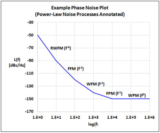
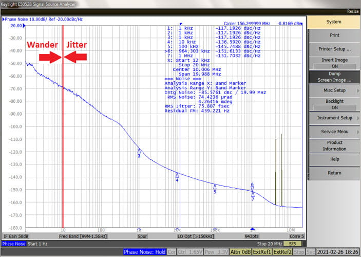
In short, this is a tabular or graphical plot of L(f) [script ell of f]; the noise power in one phase modulation sideband versus carrier power, at frequency offsets from the carrier. For example, -70 dBc/Hz at 100 kHz and –150 dBc/Hz at 20 MHz. The dBc/Hz units refer to power in dB relative to the carrier power per Hertz of bandwidth. Phase noise is typically measured using a phase noise analyzer or a spectrum analyzer with a phase noise option.
Often shown on the same plot are non-random short-term clock phase fluctuations referred to as spurs or spurious. These spurs, depicted as discrete components, have units of dBc.
As with other systems analyses, we will generally find it easier to understand clock devices and clock distribution networks or clock trees in the frequency domain. (I plan to cover phase noise and spurs in more detail in a subsequent post.)
The Role of Jitter Attenuators
It’s not uncommon to have to work with (or at least start with) relatively noisy or jittery clocks. These can arise for a number of reasons. For example, when the clock is:
• recovered from a serial data stream
• sourced from a noisy IC such as an FPGA or a noisy PC Board
• derived from a TCXO or OCXO with good wander specs that is otherwise jittery
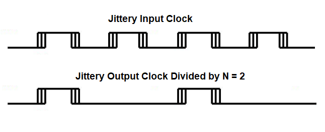
• "gapped" meaning that for synchronization purposes there are missing edges
In such cases, we need a particular type of clock device, a jitter attenuator or "jitter cleaner", to attenuate or minimize phase noise and spurs over the offset frequencies of interest. The resulting output clock is then distributed to the devices that need its improved jitter performance.
The distinguishing characteristic of Jitter Attenuators is that they are essentially narrowband Phase Locked Loops (PLLs) with a "low pass" jitter transfer function. That is these devices attenuate jitter components whose frequencies are greater than the PLL's loop bandwidth (BW). Modern jitter attenuators often have programmable loop BWs over a wide range, from as low as 0.1 Hz to as high as 1 or a few kHz.
By contrast, another category of clock chip, the clock generator, is a wideband PLL used primarily for clock multiplication from a low jitter source. These devices usually have fixed loop bandwidths on the order of 100s of kHz to 1 MHz.
The Measurement Problem
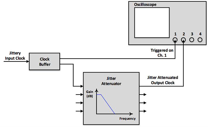
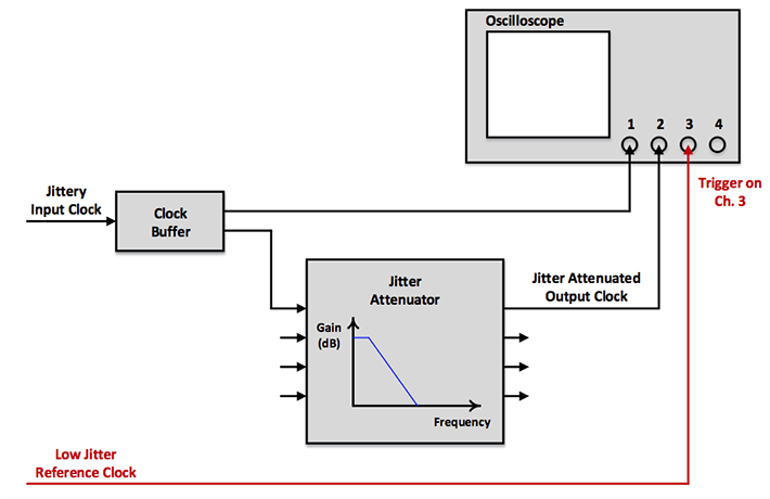
So what's the problem? Well, every so often a customer will contact us and write something like 'We're testing one of your clock chips and comparing the output clock versus the input clock and it seems surprisingly jittery'. Invariably we will find that the test set-up boils down to something like the following where the oscilloscope is being triggered by the jittery input clock.

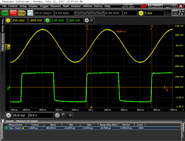
The result will often look similar to that shown in the figure below. In this example the jitter attenuator is an Si5347 with loop BW = 100 Hz. The top yellow trace is the input clock which is a 25 MHz sine wave from a signal generator with 1 kHz FM, 100 Hz deviation applied. The bottom green trace is the output clock which is also 25 MHz just to keep things simple.

Shouldn't the output clock be less jittery? Is it jitter attenuated or not? This is the case of the (apparently) jittery jitter attenuated clock.
Given the measurement set-up shown earlier, three factors must be present to observe this apparent mystery:
• The input clock is jittery.
• The output clock is less jittery. In other words, the jitter attenuator is doing its job.
• The output clock is being triggered by (compared to) the input clock.
Now you should be able to recognize the basic problem even if disguised in a more complicated application.
Note that if you triggered on the output clock then the input clock would look jittery by comparison. See below. Which clock appears jittery then is just a question of trigger perspective. This particular scope measurement is not conclusive without knowing which clock was more jittery a priori.

Diagnosis by Loop Bandwidth
You can obtain some insight as to what's really going on with this particular test configuration by playing with the Jitter Attenuator's loop bandwidth. Try narrowing and widening the BW and then observing the results on the scope.
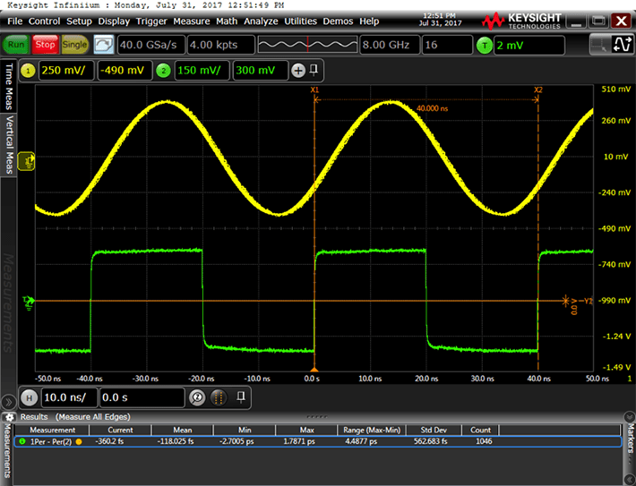
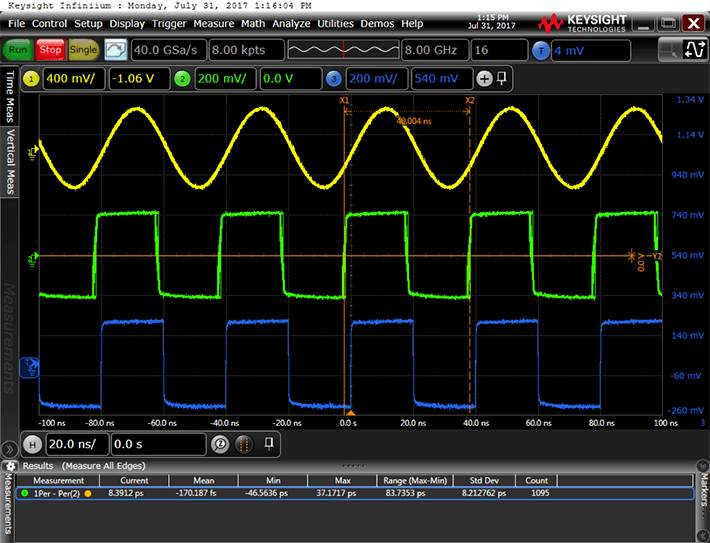
Assuming a jittery input clock, you should generally see that widening the BW makes the output clock appear less jittery versus the input clock. This is because widening the BW means the PLL will track the input clock more, jitter and all. In Figure 4 below, the Si5347’s loop BW has been widened to 4 kHz. There is essentially no jitter attenuation and the output clock does not appear jittery compared to the input clock.

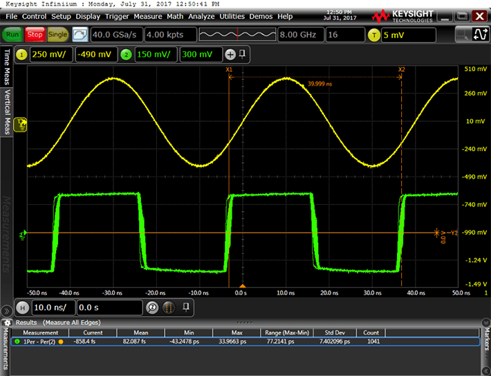
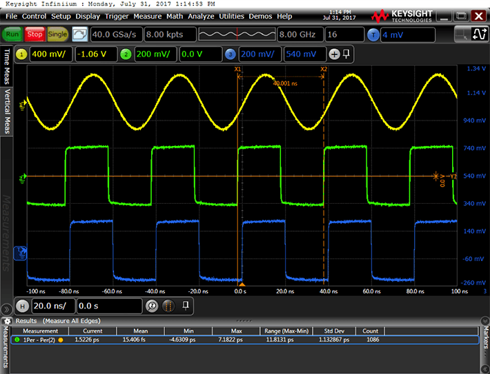
Conversely, narrowing the BW makes the output clock appear more jittery versus the input clock. That's because a narrower loop BW corresponds to more jitter attenuation. Ironically, it is the very success of the jitter attenuator in this test configuration that is the root cause of the apparent mystery. If the output clock simply tracked the input clock then the trigger source would be irrelevant. In the figure below, the Si5347’s loop BW is narrowed back down to 100 Hz.

A jitter attenuated clock is generally different from its jittery input clock, above and beyond any frequency scaling. If its spectrum has significantly changed, this should be relatively obvious when measuring and comparing the phase noise of each clock. However, as I mentioned before, this takes specialized equipment such as a phase noise analyzer or a spectrum analyzer with a phase noise option.
Third Party Arbitration
OK, so what's a better way to simultaneously compare the jittery input and jitter attenuated output clocks if all you have is a scope? Find a third party to arbitrate. In other words, find or generate a low jitter reference clock integer-related and synchronous to both the input and output clocks. Then use this reference as the trigger for both the input and output clocks. See the revised test set-up diagram in the figure below. Now you can clearly and fairly compare the jitter of the input and output clocks simultaneously in the time domain.

Here are a couple of example plots in which all the oscilloscope traces are 25 MHz as before. The top yellow trace is the jittery (frequency modulated) input clock and the middle green trace is the jitter attenuator’s output clock. The bottom blue trace is the new low jitter reference clock being used as the trigger. In the first instance, in the figure below, the jitter attenuator’s loop BW is 4 kHz and the output clock is fairly jittery just like the input clock.

In the second instance, in the figure below, the jitter attenuator’s loop BW is 100 Hz and the output clock is much less jittery. In this particular example, the standard deviation of the jitter attenuated clock’s cycle to cycle jitter dropped from 8.2 ps to 1.1 ps when the loop BW was decreased from 4 kHz to 100 Hz.

Conclusion
I hope you have enjoyed this first Timing 101 article and, if you are new to the field, that you won't be caught off guard should you run in to this scenario.
Some of the subjects I hope to cover in later installments include a deeper dive in to jitter, phase noise, clock trees, wander, and output clock formats. If you have topic suggestions, or there are questions you would like answered, appropriate for this blog, please send them to kevin.smith@skyworksinc.com with the words Timing 101 in the subject line. I will give them consideration and see if I can fit them in. Thanks for reading.
Keep calm and clock on. And click here for more information.
[Note: This blog article was originally posted online in August 2017. It has been lightly edited, and updated to reflect Skyworks Solutions’ acquisition of Silicon Labs’ Infrastructure and Automotive business, completed on July 26, 2021. The Timing 101 series continued for 12 articles and was superseded by the Timing 201 series.]

By Kevin G. Smith
Sr. Principal Applications Engineer


